Software developers know that their products do not exist in a bubble. All of their design capabilities, limitations, and general guiding principles are governed by the environment in which they intend their product to run. When getting ready for application deployment, they must be sure that their platform is not only compatible with the latest architecture but that it is prepared to take full advantage of the resources at its disposal.
Navigating this element of the design process can be tricky. It involves diligent research of the latest processing architecture along with knowing which new changes lie on the horizon. At least they do not have to go it alone. Leading companies like Intel and their IoT Solutions Alliance partners like UNICOM Engineering can make anticipating system demands and adapting to new features easier.
This three-part guide will help you gear up for the current demands of the market in light of Intel’s new Haswell architecture and the “Broadwell” 14nm fabrication node versions. Read on to see an overview of what the new Intel chips have in store for you and your customers, along with how your design process should respond accordingly.
The Benefits of Intel’s Haswell Microarchitecture
Intel Haswell microarchitecture was built with modern performance demands in mind. Enterprise-level networking systems are now seeing more demand than ever for memory and bandwidth. Developments like the Internet of Things (IoT) are further increasing throughput, putting a strain on aging processor designs.
A key improvement in the Intel Xeon E5-2600 v3 processors based on Haswell microarchitecture for server systems is a substantial increase in compute power. This will enable 40 GbE, and later 100 GbE, in standard server platforms—a tremendous benefit to address trends like IoT. With more traffic and systems to process, 40 GbE provides the ability to add more capability to systems as opposed to more servers to handle this increased traffic. This feature alone can help enterprise businesses save money.
Other key features include support for up to 14 cores as well as an integrated voltage regulator and power management system. Forecasting where the market is headed, Intel also enabled support for 4xDDR4 memory channels and socket R3 motherboard configurations.
Perhaps most significantly, DDR4 support also allows for native support of the technology’s Non-Volatile Dual In-Line Memory Modules (NVDIMM). Using this revolutionary DRAM, the processors can handle calculations using RAM similar to how it would utilize SSDs or regular HDDs. The result is a huge boost in speed for systems with the needed volume of RAM. This method of storage is also secure, providing redundancy protections in the event of a power disruption or node failure.
Additionally, Haswell-based processors can couple with PCIe access to decrease latency and greatly increase bandwidth when accessing SSDs compared to SATA or SAS.
Application Deployment with the “Tick-Tock” Model and UNICOM Engineering
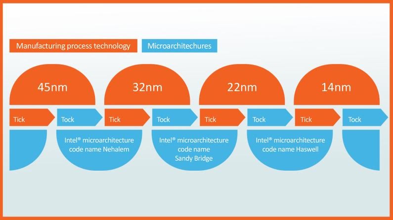
All of these changes Intel made are quite a leap forward from the previous Sandy Bridge microarchitecture. Features like Hyper-Threading and Intel’s Turbo Boost technology were built upon to add even more capability and keep pace with increasing market expectations.
While such transitions could easily be overwhelming, Intel simplifies them by alternating design cycles in their “Tick, Tock” strategy discussed in Part II.
Part III will cover how UNICOM Engineering can drive seamless platform transitions. Our experience in designing and testing platforms offers ISVs and OEMs a shortcut to market with products that take the full potential of Haswell microarchitecture and the latest features.
By reading this blog series and our corresponding whitepaper, you will be better equipped to handle the challenges that come your way as you transition to next-gen Intel microarchitecture.
Part 2: Application Deployment with the “Tick, Tock” Model
Want to Jump Ahead?
Download our FREE “Streamlining the Transition to New Intel Microarchitecture” whitepaper!
