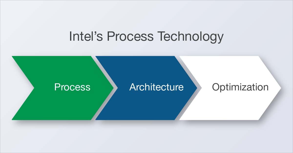
In what many saw as the inevitable, Intel announced changes to their formalized 12-month tick-tock cycle a few weeks ago. Intel has decided optimizing the current architecture with new features is a more judicious use of time than trying to overcome the financial and physical barriers of shrinking the manufacturing process further. Currently, the first “Tick” shift from the 14NM Skylake to the 10NM Cannonlake is rescheduled for launch sometime in the second half of 2017. In the meantime, the 14NM “Kaby Lake” version of Skylake is due for launch later this year, replete with new features that take better advantage of the CPU architecture’s capabilities.
Now that Intel’s grueling innovation calendar has struck a more reasonable pace, for the time being, ISVs trying to optimize their software and appliance builds for the latest CPUs can breathe a momentary sigh of relief. However, the challenge of making the most of new features will likely mandate partnerships to leverage processor technology to optimize applications while meeting performance and cost goals.
Why Deviations are Occurring in the Intel Tick-Tock Model
Intel transitioned to 14NM, but challenges to the 10NM process are causing a deviation as they determine how to keep the retail cost of the components in line with previous expectations.
These challenges come down to simple physics. As M. Mitchell Waldrop explains, processors butt up against size limits when shrunk “thanks to the heat that is unavoidably generated when more and more silicon circuitry is jammed into the same small area.” Reducing nodes below 10NM invites further complexities, such as the unpredictability of electron behavior at the atomic level.
At this time, Intel has determined that optimizing its current architecture could produce far more mileage and utility. Adding features that increase the work done per clock cycle is one preferred method, such as providing additional SIMD instruction possibilities. Intel’s acquisition of Altera adds similar functionality through efficiently structured FPGA programming logic pathways.
Updates like these allow silicon manufacturers to gain more ROI on their current processes while offering hardware and software developers more nuanced choices for maximizing performance based on application-specific workloads. They also help Intel keep pace with current hardware capabilities without having to release a whole new chipset to do it. For example, Kaby Lake boards natively support USB 3.1 ports without the use of add-on chips.
Taking CPUs Momentarily Off the Board
As Intel continues to innovate and determine cost-effective ways to produce high volumes of smaller chips, they will split their efforts — focusing on enhancing processor capabilities and overcoming 10NM manufacturing limitations simultaneously — we at UNICOM Engineering predict much of the advancements to take place outside the CPU battleground on simpler devices. DRAM and NAND memory, for instance, could become the focus of process improvements where density matters above complexity. However, even in this realm, the shift to 3D architectures makes process shifts towards smaller transistor sizes less of a priority.
UNICOM Engineering is here to help ISVs navigate technology changes and continue to stand by our promise to help ISVs determine the most optimal hardware-based appliance build path for their product’s intended environment.
Meet changes head-on, keep pace with Intel’s Tick-Tock syncopated rhythms, and maximize your development efforts. With a global value integrator and deployment partner, ambition and imagination become your only limits.
